Effect of maximizing the number of effective chips
Even if you understand the definition of the number of effective chips (the number of complete chips that can be cut from one wafer), how do you maximize it?
Isn't it usually maximized?
How much effective chips increase?
I think various questions come up.
First, let's define the chip aspect ratio and wafer placement method that will be the basis for comparison.
Now, the standard of the chip aspect ratio is a square.
There is no reason to reference a rectangle other than a square, and a square is an intuitively preferred shape.
In addition, squares are an intuitively preferred shape.
This is because if the shape is extremely slender and the long side reaches the diameter, even one chip cannot be cut out.
Therefore, it is natural to think that the opposite pole shape, square, is preferable.
Next, consider the wafer layout (determining the relative position between the chip grid and the center of the wafer circle).
If the chip shape is a rectangle (a square is one of rectangles) and the wafer shape is a circle, both are symmetrical shapes.
In this case, it is natural to choose a symmetrical position as well.
According to the information I have heard, the most common method is to select the wafer center from the chip corner and the center (two-point method).
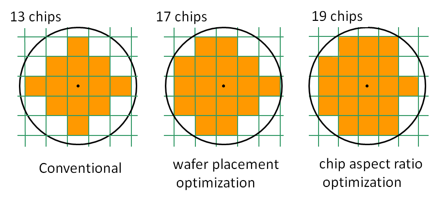
The figure on the left is an example of the reference state where the center of the wafer is placed at the center of the square chip.
In this case, the effective chip number is 13, but if the wafer arrangement is changed appropriately, the effective chip number can be increased.
Maximizing the number of effective chips by this method is called placement optimization.
The simplest method is to place the wafer at multiple locations within the chip and select the case where the number of effective chips is maximized.
Placement optimization is also quite practical with this method.
The middle diagram shows the case where the effective chip number is increased to 17 by optimizing only the wafer arrangement while maintaining the chip aspect ratio.
Furthermore, by adjusting both the aspect ratio and the wafer arrangement without changing the area of the square chip, the number of effective chips can be increased to 19 as shown in the right figure.
This is called aspect ratio optimization.
Aspect ratio optimization is a problem that adds one degree of freedom of the aspect ratio of chips to two degrees of freedom of the wafer position, which is the degree of freedom of layout optimization.
Therefore, it can be expected that the number of effective chips will be larger than the placement optimization.
However, since the chip aspect ratio can be determined by optimization in the layout design of the semiconductor, it cannot be performed after the chip shape is determined.
Also, it is unlikely that the aspect ratio can be freely selected while keeping the chip area constant in actual semiconductor layout design.
Therefore, in the case of the aspect ratio, the designer selects the feasible aspect ratio with a large number of effective chips after grasping the relationship between the aspect ratio and the effective chip number.
Effects of wafer placement optimization

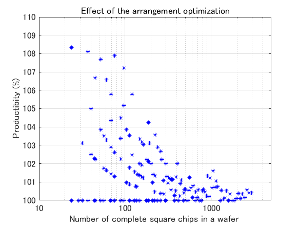
The figure on the right shows the productivity when the placement is optimized for the two-point method where either the chip center or the chip angle is selected for the wafer center.
Specifically, the horizontal axis shows the number of effective chips in a square chip with optimized wafer placement, and the vertical axis shows the ratio of the increased effective chip number by optimizing the chip aspect ratio.
When the productivity is 100%, the result of the two-point method is the best.
From this figure, when the number of effective chips is 500 or more, the effect of productivity improvement can be expected only about 0.5%.
On the other hand, if the number of effective chips is in the range of 100 to 500, an effect of about 3% can be expected, and if less than 100, an effect of about 6% can be expected.
The meaning of 100% productivity means that the result of the two-point method happens to be the optimal arrangement.
In such a case, about 25%.
Effects of chip aspect ratio optimization

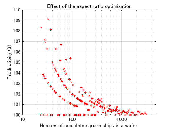
The figure on the right shows the productivity when the aspect ratio is optimized for a square chip shape, that is, a square chip shape without changing the area.
Specifically, the horizontal axis shows the number of effective chips in a square chip with optimized wafer placement, and the vertical axis shows the percentage of effective chips increased by optimizing the chip aspect ratio.
Many intuitively believe that squares are the best chip shape.
In fact, about 40% of the simulations on the right show that squares are the best.
In other words, its intuition is not a big mistake.
However, for the remaining 60%, non-square rectangles were best.
The result was also a big surprise.
The effect of optimizing the chip aspect ratio can be expected to be about 5% when the number of effective chips is less than 100, and about 1% when the number of effective chips is less than 500.
Seems small compared to wafer placement optimization.
However, the comparison target is in a state where the placement is optimized with a square chip.
If you compare it with the two-point method, it will be the sum of the effects of both the placement optimization and the aspect ratio optimization.
This is a huge productivity boost.
Usage trends
The operation of this service started in November 2017 for layout optimization and in September 2018 for aspect ratio optimization.
Placement optimization seems to be implemented in a unique way by more semiconductor manufacturers than before. Our method is the best in theory, but no user was used.
On the other hand, regarding the aspect ratio optimization, many people think that an aspect ratio of 1 is better in the first place.
In addition, since the technology can only be used in the layout design process, the number of users is not large.
For such reasons, it is not used much.
However, the number of users has been increasing gradually recently.
On the other hand, some people give up if they cannot access an external site such as our company and input semiconductor design information.
In the first place, the input values correspond only to the chip area and the values that have not yet been determined.
In addition, input invalid area, wafer diameter, orientation flat length, etc., but I do not think these values have high confidentiality.
Therefore, the fear of information leakage does not seem to exist.
If you are still worried, try selecting and entering multiple items that you do not actually use.
Easy camouflage.
 The figure on the left is an example of the reference state where the center of the wafer is placed at the center of the square chip.
In this case, the effective chip number is 13, but if the wafer arrangement is changed appropriately, the effective chip number can be increased.
Maximizing the number of effective chips by this method is called placement optimization.
