Key points of the solution
The solution of the semiconductor layout optimization and aspect ratio optimization provided on this site is described in the patent gazettes (Japanese Patent Laid-Open No. 2003-57843, Patent No. 4298571, WO2018-216091). If you are interested in the details of the solution, please see them. However, patent gazettes contain a lot of mathematical formulas, so they are not easy to read. Therefore, here we will explain the points of interest and the key points of the solution method to find the optimal solution. By doing so, you will understand the strengths and weaknesses of this solution.
Common points (finite)
 The key to the optimization used in both semiconductor layout optimization and aspect ratio optimization is the finiteization of candidate solutions.
Optimization is to select the best solution from among the candidate solutions.
If the number of candidate solutions is infinite, the true optimal solution cannot be found.
The key to the optimization used in both semiconductor layout optimization and aspect ratio optimization is the finiteization of candidate solutions.
Optimization is to select the best solution from among the candidate solutions.
If the number of candidate solutions is infinite, the true optimal solution cannot be found.
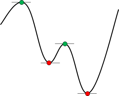
However, if the candidate solution is finite, the optimal solution can always be selected. The figure on the right is drawn to show an example of finiteization. Then, find the minimum value from this curve.
In this case, the length of the curve is finite, but the curve is continuous, so the points on the curve are infinite. In other words, if you search without any conditions, the number of times will be infinite. However, given that the first derivative is zero, the candidate solution is narrowed down to four points, red and green. In addition, if we add the condition that the second derivative is positive, it will be red two points from the beginning. This is finiteization. If you make it finite, you do not need to compare it to infinity, so you always find the optimal solution. This finiteization is the key to the optimal solution.
Key points of wafer placement optimization
 You can see that finite candidate solutions are the key to the optimal solution.
Let's consider the optimal solution for wafer placement.
What if there are infinite candidate solutions?
You can see that finite candidate solutions are the key to the optimal solution.
Let's consider the optimal solution for wafer placement.
What if there are infinite candidate solutions?
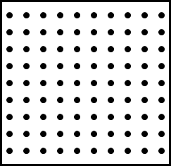
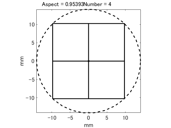
Perhaps if you put a lot of candidate points in a chip at the center of the wafer, you will try to count the effective chips. For example, aren't the candidate points distributed at equal intervals as shown in the right figure? The reason is that the narrower the interval and the higher the number of candidate solutions, the better the solution can be expected. However, even if the number of points is increased infinitely, it does not prove to be truly optimal. This is because the area where the solution exists is not a point but a surface, and there are infinite candidate solutions.
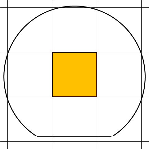 Therefore, consider the example shown in the figure on the right.
In this case, there is only one active chip (yellow).
However, moving the wafer up a small amount increases the number of active chips to two.
If you move left and right, the number of effective chips will be three.
If the wafer center is superimposed on the chip grid point, the number of effective chips will be four.
Therefore, consider the example shown in the figure on the right.
In this case, there is only one active chip (yellow).
However, moving the wafer up a small amount increases the number of active chips to two.
If you move left and right, the number of effective chips will be three.
If the wafer center is superimposed on the chip grid point, the number of effective chips will be four.
In other words, one chip can be divided into multiple areas with different numbers of effective chips. By the way, what happens when the number of effective chips increases or decreases? There, the wafer boundaries intersect the chip grid points. As the number of effective chips increases, the chip grid points that cross the wafer boundary move into the wafer. Conversely, when the effective chip count decreases, the chip grid point moves outside the wafer boundary.
Now, let's translate the wafer with one chip grid point on the wafer boundary. Then, another chip lattice point crosses the wafer boundary line. The number of effective chips increases if the grid points outside the wafer boundary enter the inside of the wafer boundary after crossing. Conversely, it will decrease.
What is important here is that when the two chip grid points are on the wafer boundary, the effective chip count is on the boundary. In other words, the candidate solution can be finite by using the condition that the two chip grid points are on the wafer boundary.
Key points of chip aspect ratio optimization
 Aspect ratio optimization is a three-degree-of-freedom optimization problem that adds two degrees of freedom for wafer placement and one degree of freedom for chip aspect ratio.
The optimization information to be presented is the maximum number of effective chips at the time of layout optimization corresponding to the chip aspect ratio.
If it is displayed in a graph, the horizontal axis is the chip aspect ratio, and the vertical axis is the number of effective chips for placement optimization.
Aspect ratio optimization is a three-degree-of-freedom optimization problem that adds two degrees of freedom for wafer placement and one degree of freedom for chip aspect ratio.
The optimization information to be presented is the maximum number of effective chips at the time of layout optimization corresponding to the chip aspect ratio.
If it is displayed in a graph, the horizontal axis is the chip aspect ratio, and the vertical axis is the number of effective chips for placement optimization.
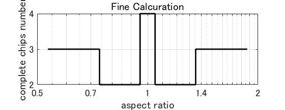
When the aspect ratio changes, the graph becomes a line graph in which the number of effective chips changes stepwise at a specific aspect ratio. The figure on the right is an example. As you can see, if the aspect ratio at which the maximum number of effective chips changes and the number of effective chips there are known, no other information is needed. In other words, finding the aspect ratio at which this breakpoint occurs is the finiteization of the candidate solution.
 In the aspect ratio optimization, not only the chip aspect ratio but also the x and y coordinates of the wafer position can be adjusted.
Under such conditions, consider the phenomenon that the number of effective chips increases or decreases due to the change in the aspect ratio.
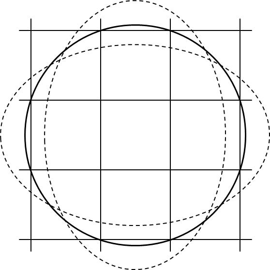
Even if the center position of the wafer is adjusted, the effective number of chips will change if the aspect ratio is changed to either large or small.
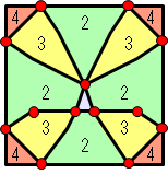
In such a case, multiple chip grid points should be on the wafer boundary circle.
So how many chip lattice points are on the wafer boundary circle?
With up to two chips, the state of contact with the wafer boundary circle can be maintained even if the chip aspect ratio is changed.
Even if there are three, if the center of the wafer is not included in the triangle made by those three points, it seems to be OK.
But this is the limit.
When at least three of the chip grid points intersect the wafer boundary line and the center of the wafer is included inside the polygon connecting these intersection points, the change in the aspect ratio will increase or decrease the number of effective chips.
For example, in the case of the upper right figure.
In the aspect ratio optimization, not only the chip aspect ratio but also the x and y coordinates of the wafer position can be adjusted.
Under such conditions, consider the phenomenon that the number of effective chips increases or decreases due to the change in the aspect ratio.
Even if the center position of the wafer is adjusted, the effective number of chips will change if the aspect ratio is changed to either large or small.
In such a case, multiple chip grid points should be on the wafer boundary circle.
So how many chip lattice points are on the wafer boundary circle?
With up to two chips, the state of contact with the wafer boundary circle can be maintained even if the chip aspect ratio is changed.
Even if there are three, if the center of the wafer is not included in the triangle made by those three points, it seems to be OK.
But this is the limit.
When at least three of the chip grid points intersect the wafer boundary line and the center of the wafer is included inside the polygon connecting these intersection points, the change in the aspect ratio will increase or decrease the number of effective chips.
For example, in the case of the upper right figure.
 The finite number of candidate solutions in chip aspect ratio optimization is to find the wafer center position and aspect ratio that satisfy this condition.
In the placement optimization, we looked for a case where two chip grid points touched the wafer boundary.
Similarly, aspect ratio optimization looks for three chip lattice points touching the wafer boundary.
The difference from the placement optimization is that the center of the wafer is included inside the triangle connecting the grid points (including on the sides).
The finite number of candidate solutions in chip aspect ratio optimization is to find the wafer center position and aspect ratio that satisfy this condition.
In the placement optimization, we looked for a case where two chip grid points touched the wafer boundary.
Similarly, aspect ratio optimization looks for three chip lattice points touching the wafer boundary.
The difference from the placement optimization is that the center of the wafer is included inside the triangle connecting the grid points (including on the sides).
However, you notice another problem here. Changing the aspect ratio changes the position of each grid point. The amount of movement is proportional to the distance from the center of the wafer boundary circle. In the placement optimization, the chip lattice point does not move, so we only need to optimize the wafer center position. But this time, I could not come up with a solution algorithm.
Therefore, we considered a method of solving without changing the chip grid. Instead of changing the chip grid, it changes the aspect ratio of the wafer boundary circle. In other words, the wafer boundary circle is made elliptical. Then, translate it so that it touches the three selected grid points. The equation solves a system of quadratic equations where the ratio of the major and minor axes of the ellipse and the two-dimensional coordinates of the center of the ellipse are unknown. In reality, the wafer cannot be deformed freely. However, as a problem, it is converted to an equivalent mathematical expression and solved, and then inversely converted to a correct solution.
How to use To the previous page
To the next page FAQ
Click here for your opinion. Click here for questions. Feel free to help yourself.
(Update Oct 29, 2023)